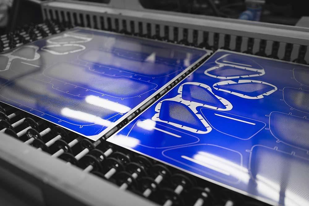
Photo etching, also known as chemical etching or photochemical machining, is a highly precise, cost-effective metal machining process used to produce complex components from a wide range of metals. This technique is especially useful for producing fine details, small holes and slots in thin-walled parts.
The photo etching process begins with the creation of a photoresist mask, which is used to protect the areas of the metal that will remain intact during the etching process. The exposed areas are then chemically etched away until only the desired shape remains. Photo etching can be performed using either liquid or vapor phase chemicals depending on the desired depth of penetration.
Electronics manufacturing – Photo etching is used to create printed circuit boards (PCBs). The PCBs are made by applying a layer of copper onto an insulating substrate material such as fiberglass or plastic, leaving openings for electrical connections through which current flows between components such as transistors and capacitors. Photo etching is used to create these patterns so that they are precise down to fractions of a millimeter across large areas.
Medical devices – Photo etching allows medical device manufacturers to create precise openings within metal casings that allow access
Photo chemical etching is a photochemical process that uses a combination of light and chemistry to selectively remove materials from a surface. In an etching process, one or more of the components in the surface coating is soluble in an etchant and remains after exposure to light but not darkness. This article provides details on photo chemical etching for PCBs. Readers should also see Chemical Etching of Copper and Other Metal Surfaces, which has details on other types of chemical etching processes used for copper and metal substrates.
Most PCBs are made by electroplating copper on both the top and bottom of a porous substrate. Photo Chemical Etching is a process used to etch away the copper on the bottom of the board, leaving only the copper on the top. This is done after all the board patterns have been made using photoresist (chemical-resistant material coated on a board and exposed to light to make patterns). In order to make PCBs, it is necessary to have copper on both sides of the board so that connections can be made. However, only the top copper is used to make the circuit connections. The bottom copper is not used but it has to be there in order to make the connections. Therefore, Photo Chemical Etching is used to remove the bottom copper so that the substrate is left. Using the top copper alone makes a board that is only one-sided.
The process used in PCB photo etching is often the same process used for the chemical etching of copper and other metals. Often, however, photo etching is used on non-conducting materials such as ceramics. When a material is etched, a chemical reaction occurs with the surface of the material. These chemicals are generally acids or bases (also known as etchants). When these etchants come in contact with the surface of the material, chemical reactions occur. Once the surface is damaged, the material can be removed. For photo etching, a light-sensitive coating is applied to the surface of the material. This coating can be made of either a photosensitive liquid or a dry chemical. Once this coating is applied, the surface is exposed to light through a photoresist coating.
Materials used in photo etching are generally the same as those used in chemical etching. In some instances, however, other types of materials may be used. - Photoresist - A chemically resistant material used as a coating on a board to protect the copper while a pattern is being developed. - Copper - Copper is used on the top side of the board as a conductor. It is also used on the bottom side of the board as a base for the etchants. - Solvents - Solvents are used in the chemical etching process. They are used to dissolve the etchant.
- The etch is selective, etching only the copper on the bottom of the board, leaving the top copper untouched. - There is no need to remove the photoresist from the board after it has been exposed. - The process is environmentally friendly because it does not use harmful compounds such as chlorine.
- The process is very time consuming, taking up to 24 hours. - There are limitations on the size of the board that can be photo etched. Boards that are too large or too small cannot be etched by the process.
- Boards should be larger than 1 sq. ft. so that they can be moved while they are being exposed to the light. Boards smaller than 1 sq. ft. are not big enough to be moved and must remain stationary while they are being exposed to the light. - The exposure time should be increased as the thickness of the board increases. - The exposure time should be decreased as the thickness of the board decreases.
It is important to know about the advantages and disadvantages of procedures such as photo chemical etching. This will help the reader understand how the process works and if it is the best etch for their application. Because photo etching takes up to 24 hours, it should be planned in advance. It is important to know when the order must be received, when the board must be etched, and how long it will take to etch the board. During the etching process, monitoring the etchant level, temperature, and pressure will help to improve the process. This information can be found in the manufacturer’s user manual.
